Scaling Semiconductor Performance: Innovations in High-Performance Computing
“High performance compute” in the semiconductor context refers to specialized chips designed to handle extremely complex calculations and large data sets at very high speeds, requiring advanced chip architectures and manufacturing processes to achieve maximum performance. Areas like machine learning, weather forecasting, genomic analysis, and advanced simulations heavily rely on high performance computing chips. Optimizing factors like transistor density, cache size, memory bandwidth, and interconnect design are crucial for achieving high performance. New techniques like 3D stacking and chiplet design are being used to further improve performance and power efficiency in high performance computing chips.
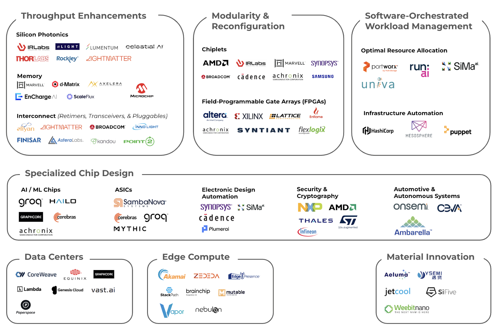
It is best to contextualize this discussion within the basic architecture of a server rack:
Chips:
The substrate is a thin, circular slice of crystalline material (typically silicon wafer)
- Areas of the substrate are doped with impurities (like phosphorus or boron) to create regions of n-type or p-type conductivity
- Tiny MOSFET (Metal-Oxide-Semiconductor Field-Effect Transistors) layers are built on the substrate to switch and amplify electrical signals
- Thin films of metal (copper or aluminum) connect transistors
- Layers of insulating material (like silicon dioxide or low-k dielectrics) prevent electrical interference between metal layers
- The fabricated semi circuit is cut into individual dies (chips) from the wafer.
- Each die is enclosed in a protective package made of plastic, ceramic, or epoxy resin to shield it from physical damage and environmental factors
- Fine gold or copper wires connect the chip to the package pins or leads
PCB (Printed Circuit Board) Integration
- Packaged chips are mounted on PCBs, which may include connectors and additional components such as resistors, capacitors, and voltage regulators
- Heat sinks or integrated cooling systems are attached to manage thermal dissipation during operation
Rack-Level Systems
- Racks are large steel frames housing multiple server units containing PCBs, chips, and storage systems
- Boxes or Units are modular units that hold the semiconductor-containing boards. These boxes may include: power supplies, cooling systems, networking interfaces and redundancy features
Chiplet Technology
“Scale-Up Technology” happens intra-rack, and thus refers to any interconnections, memory and compute access within a single rack. These are innovations in powerful processors and accelerators to boost performance within individual systems. “Scale-up” refers to the fastest way to amplify compute power over short distances within a rack. For NVIDIA, this is handled by NVLink72, which connects GPUs to make them behave as one single, powerful GPU. The current limit for scale-up is about 256 GPUs (or 8 GPUs across 32 units in a rack).
Scale-Up Technologies include
- Silicon Photonics
- Memory Technology
- Chiplet Technology
Silicon Photonics captured public interest in the 2000s but did not begin commercializing till the 2010s. Today photonics play a critical role in meeting the demand for higher-speed data transfer and lower energy consumption in cloud computing. Photonic Integrated Circuits (PICs) are semiconductor devices that integrate multiple optical components, such as lasers, waveguides, modulators, and detectors, onto a single chip. They perform functions similar to electronic integrated circuits (ICs) but use photons (light) instead of electrons to process and transmit information.
PICs use light to transmit data, enabling high-speed, low-latency, and energy-efficient communication compared to traditional electronic circuits.
Benefits of Photonics:
- Light can carry more data over wider bandwidths compared to electrical signals.
- Optical communication generates less heat, leading to greater energy efficiency.
- Compact design and integration reduces the physical size and complexity of optical systems.

Ayar Labs is a Leader in Silicon Photonics
Ayar Labs and Celestial Labs are two startups which are prominent in the market for utilizing silicon photonics, transmitting data using laser light instead of wires, allowing data transfer to reach the speed of light. Lightmatter (which raised a $400 million Series D in October 2024) builds photonic processors for AI and machine learning workloads, aiming to surpass the performance and efficiency of traditional electronic processors. Rockley Photonics focuses on PICs for healthcare applications, such as non-invasive glucose monitoring.
Memory technology plays a pivotal role in scaling up semiconductor performance, particularly for AI and machine learning (ML) applications that demand high-speed data processing. Players like Marvell and Microchip provide commodity-based memory solutions similar to Samsung and Micron, leveraging DRAM (dynamic random access memory) and SRAM (static random access memory) configurations. DRAM, known for its higher density and lower cost, serves as the backbone for most memory-intensive operations, while SRAM’s faster access speeds, maintained through constant charging, make it ideal for high-speed caches. Emerging players such as ScaleFlux differentiate themselves by introducing innovative memory solutions tailored for specific high-performance workloads, pushing the boundaries of memory efficiency and customization. Stacked memory architectures on boards are now commonplace, optimizing both footprint and performance for various computational needs.
In-memory computing has reshaped the semiconductor landscape by integrating processing and memory functions into the same unit. This technology eliminates the need for frequent data movement between processors and memory, reducing latency and power consumption—key considerations for AI/ML scalability. Startups at Series A stage – Axelera AI, EnCharge AI, and D-Matrix – are powering this innovation. Axelera AI’s multicore in-memory computing platforms enhance efficiency for edge AI solutions, while EnCharge AI emphasizes scalability for dense edge AI applications. D-Matrix, focusing on large-scale AI workloads, applies digital in-memory computing for data center acceleration. The existence of these companies signals the strategic importance of in-memory technologies for advancing AI hardware performance.
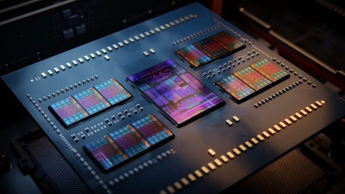
Chiplet technology represents a paradigm shift in semiconductor design, allowing manufacturers to integrate multiple smaller chip components, or chiplets, into a single cohesive package. This approach bypasses the scaling limitations of monolithic chips, enabling greater functionality and performance within the same physical space. Advanced interconnect standards, such as UCIE (Universal Chiplet Interconnect Express) and silicon bridges, facilitate high-speed communication between chiplets, ensuring seamless integration. Companies such as AMD have pioneered this approach with their EPYC processors, which use chiplets for CPU cores and cache to deliver exceptional compute power for data centers and high-performance computing. Startups such as IR Labs are innovating further by developing chiplets designed to sit in server racks alongside GPUs, employing cutting-edge interconnect technologies, including laser communication, to expand immediate memory access and enhance system efficiency.
By integrating standardized communication protocols, chiplet technology also supports Scale-Out architectures (more on this below), where distributed systems work cohesively to process large workloads. The continued evolution of chiplet technology promises to redefine system design, delivering faster and more flexible hardware.
Scale-out technologies operate at a rack-to-rack level, connecting entire racks through top-of-rack switches to create a cohesive, high-performance network. Unlike scale-up approaches that enhance individual components, scale-out involves solutions that enhance the performance and capacity of computing systems by distributing workloads across multiple interconnected systems. These technologies focus on modularity, parallelism, and efficient communication between systems. The systems are underpinned by advanced graph theory to manage parallel workloads and ensure recovery in case of failure.This type of scaling is essential for AI training, which demands as much compute power as possible to halve training times by doubling available compute.
Here’s a breakdown of the main types of scale-out technologies:
- Interconnect Technologies
- Software-Orchestrated Workload Management
- Specialized AI Chips
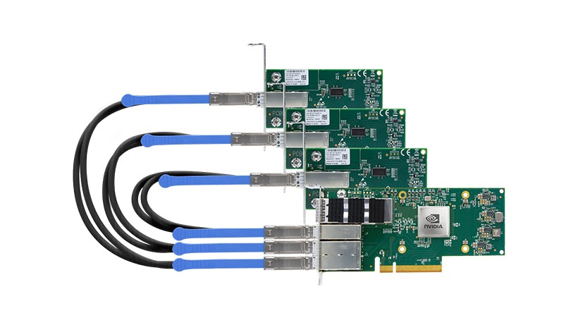
NVIDIA’s Infiniband Adaptors
Interconnect technologies enable seamless high-speed data transfer between nodes in data centers, HPC clusters, and advanced computing systems. These technologies, such as InfiniBand for low-latency networking, Ethernet (100G/400G/800G) for scalable connectivity, and NVIDIA’s NVLink/NVSwitch, play a critical role in reducing latency and improving system efficiency. Compute Express Link (CXL) and other emerging standards further enhance shared memory access across CPUs, GPUs, and accelerators.
Eliyan – which raised $40M in Series A from Intel Capital and Micron Ventures – develops high-performance chiplet interconnects for multi-die integration. Lightmatter and Celestial AI focus on photonic interconnects to accelerate data transfer, leveraging light for energy-efficient, high-bandwidth communication. GV-backed Lightmatter creates photonic interconnects to accelerate data transfer within and between chips using light-based technology. Avicena employs microLED-based interconnects to improve chip-to-chip communication. AMD’s acquisition of Pensando for $300M underscores the importance of programmable processors (DPUs) that enhance networking, security, and storage functions, further optimizing interconnect performance in data centers.
Software-Orchestrated Workload Management refers to platforms that manage distributed systems to ensure efficient workload distribution and scaling. This segment involves software solutions that automate the scheduling, execution, and monitoring of workloads across diverse computing environments. These tools ensure optimal resource utilization, scalability, and reliability by managing complex workflows, dependencies, and data flows. For enterprises handling large-scale data processing and cloud services, these tools are essential.
Imagine a large restaurant kitchen during a busy dinner service. The head chef (software orchestrator) assigns tasks to the cooks, ensuring each dish is prepared in the right order and on time. Some dishes need to be cooked simultaneously (parallel tasks), while others require one step to finish before the next begins (dependencies). The head chef also ensures no one is overloaded and that ingredients (resources) are used efficiently without waste. If a new large order comes in, the chef adjusts the workflow to accommodate it seamlessly.
Similarly, in computing, software-orchestrated workload management ensures that servers and systems work together efficiently, distributing tasks, managing dependencies, and scaling resources to handle varying workloads, just like the head chef managing the kitchen. For example, tools such as Kubernetes orchestrate cloud applications by ensuring that different parts of a program (like storing data, processing requests, or running computations) are allocated to the right servers and work harmoniously.
One such example is Portworx (acquired by Pure Storage), which offers cloud-native storage and data management solutions for Kubernetes to facilitate efficient workload orchestration across distributed systems. A16z and Khosla-backed D2iQ (previously Mesosphere), offers a platform for automating the operation of containerized and data-intensive applications across cloud and data center environments.
Specialized AI chips have been fashioned by startups to address scale-up and scale-out needs simultaneously. For instance, Mythic develops analog AI processors for edge devices, delivering high-performance AI inference with low power consumption, suitable for IoT and edge applications. Cerebras designs wafer-scale AI processors to accelerate deep learning and AI workloads, offering unparalleled performance for training and inference tasks.
Neural Processing Units (NPUs) are specialized processors designed to accelerate artificial intelligence (AI) and machine learning (ML) tasks. They are optimized for handling the parallel processing requirements of neural networks, offering enhanced performance and energy efficiency compared to general-purpose CPUs or GPUs. For instance, Quadric develops general-purpose NPUs that combine high ML inference performance with the ability to run complex C++ code, simplifying system-on-chip (SoC) designs. DEEPX is a South Korean startup developing on-device AI chips (NPUs) for various applications, including autonomous vehicles and smart devices.
Retimers, Transceivers, Pluggables
Neither strictly scale-up nor scale-out technologies, Retimers, Transceivers and Pluggables connect parts in a box. These technologies focus on throughput rather than networking algorithms.
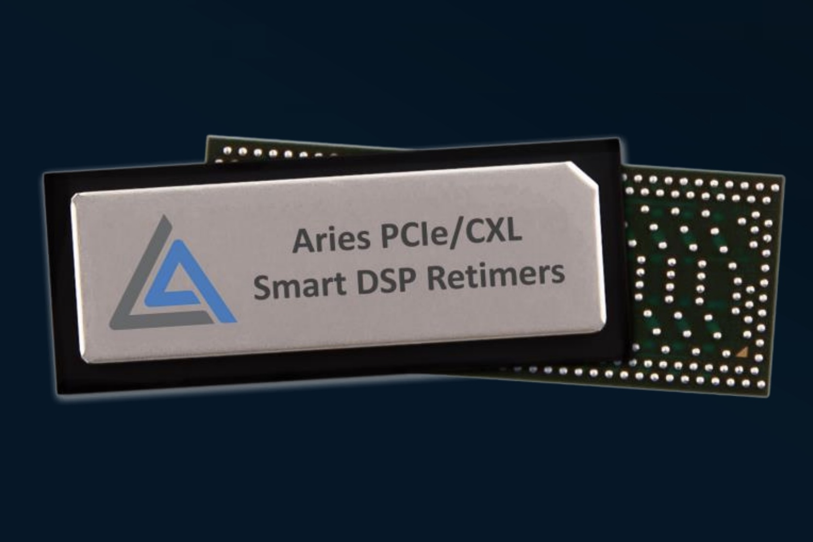
Retimers are specialized chips or integrated circuits. They enhance signal integrity (clean up and amplify electrical signals as they traverse high-speed communication links), reduce noise and jitter (ensure data signals maintain quality over longer distances or complex interconnects), enable high data rates (support next-generation protocols by overcoming physical limitations in signal transmission).
In a Scale-Up Context, Retimers play a supportive role by ensuring high-bandwidth, low-latency communication within a single system, e.g. enabling faster data transfer between a processor and memory/storage components within a server or AI accelerator system. In a Scale-Out context, Retimers are critical for inter-system communication in scale-out architectures, where multiple nodes (servers, GPUs, or storage systems) are networked together, e.g. improving the reliability of high-speed links in distributed data centers or between edge devices and central servers.
Astera Labs first developed retimers to amplify signals in long-distance cables. Astera’s innovation lay in optimizing light transmission, adjusting to narrower wavelength increments or using multiple colors to improve signal clarity. Similarly, Kandou offers high-speed, energy-efficient connectivity solutions, including USB4 retimers, to enhance signal integrity in data transmission.
Tranceivers and Pluggables work with Retimers. A transceiver is a device that combines a transmitter (Tx) and a receiver (Rx) into one unit. It transmits data via optical fibers by converting electrical signals into light and receives optical signals which it converts back into electrical signals. Finisar (now part of II-VI) is a leading manufacturer of optical transceivers. Broadcom also offers transceivers for various optical communication standards.
Pluggables are a specific form factor of transceivers designed to be hot-swappable, meaning they can be easily inserted or removed from networking hardware like switches and routers without shutting down the system. They provide modular, scalable networking capabilities by allowing users to upgrade or replace optical modules as needed. InnoLight is one innovator in pluggable modules for data centers.
Transceivers and pluggables are primarily optical components for long-distance communication, while retimers are electrical components focused on maintaining signal integrity over shorter distances. They complement each other in building high-speed communication systems.
By integrating retimers, transceivers, and pluggables, companies aim to provide cost-effective upgrades to existing infrastructure, appealing to data centers looking to handle increasing workloads and traffic demands efficiently. Proponents of this strategy see it as a logical and scalable way to upgrade data centers without a complete overhaul, offering cost and energy efficiency. But this has been met with mixed reception. Some in the industry argue that this approach is overly focused on incremental improvements and does not address long-term architectural challenges, such as shifts to newer interconnect standards or full-stack rethinking for AI-driven workloads.
—————————————–
If you are a builder, investor or researcher in the space and would like to have a chat – please reach out to me at ayla@thelotuscapital.com
